2.5D Current Distribution in a Multilayer PCB - QuickField simulation example
The example is based on the high-current battery - connection of the Texas Instruments
bq78PL114 evaluation board. The illustration below is for illustrative purposes only and shows a typical
battery-management PCB containing the section modeled in QuickField.
How to calculate DC current distribution in multilayer PCB traces connected by vias?
Answer Typical applications Geometry
Given
Task
Solution Results ReferenceEngineering question
Model each copper layer as a separate plane-parallel QuickField DC Conduction region and couple the layers through common via potentials calculated by the QuickField PCB 2.5D Current Flow Solver.
high-current PCB interconnects, battery management boards, power distribution modules, multilayer copper buses
Download
Simulation problem
Plane-parallel problem of DC conduction.
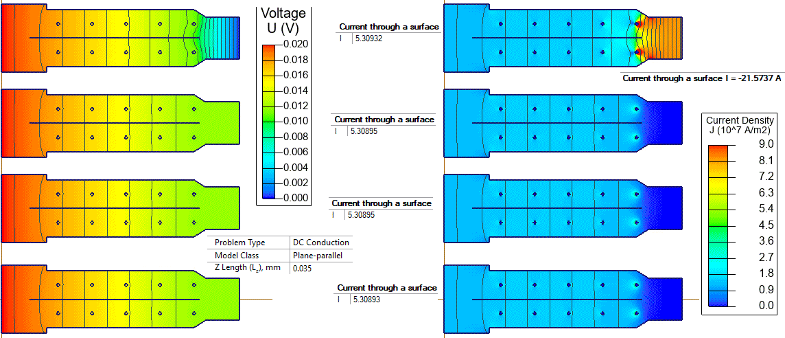
The modeled section is represented by four identical copper layers connected by ten stitching vias.
The copper path is approximately 42 mm long and 12 mm wide. Bttery voltage is applied at the left end on all four layers.
The R3 pad terminal is applied only on the top layer at the right end.
Potential of R3 pad terminal: 0 V;
Potential of battery terminal: 20 mV (the voltage drop imposed across this PCB segment under load, not the actual battery pack voltage);
Copper conductivity: 58 MS/m;
Copper thickness: 35 µm on each layer;
Number of physical vias: 10.
Calculate the current redistribution between the four PCB layers and determine the currents passing through the stitching vias.
Each PCB layer is modeled as a separate 2D current flow region.
For every physical via, the corresponding boundaries on all participating layers are assigned a common unknown potential.
A Python script automatically adjusts these via potentials until the algebraic sum of currents through each physical via becomes zero.
The current initially spreads among the four parallel copper layers and then transfers back to the top layer near the R3 pad terminal.
The vias closest to the R3 pad carry the largest interlayer currents.
The coupling matrix has full rank, and the solution converges after two matrix-correction iterations.
The QuickField model geometry is adapted from Texas Instruments,
bq78PL114 System Design Guidelines,
Application Report SLUA537, Figures 18–21. The board illustration on this page is an original simplified redraw prepared for the QuickField example.
Related examples